Hotspot prediction: SEM image generation with potential lithography hotspots
- Journal
- IEEE Transactions on Semiconductor Manufacturing
- Volume
- 37
- Page
- 103-114
- Year
- 2024
- Date
- 2024-02-01
- Link
- https://ieeexplore.ieee.org/document/10297297 500회 연결
Abstract
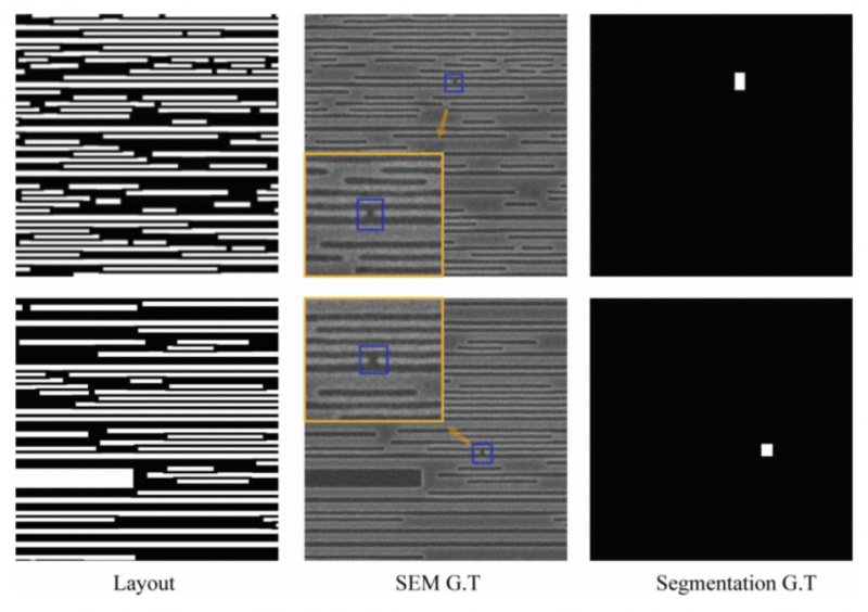
Since the invention of transistors and integrated circuits, the development of semiconductor processes has advanced rapidly. Current microchips contain hundreds of millions of transistors. The remarkable development of semiconductors thus far has also led to difficulties in designing tightly packed lithography patterns without unwanted defects called hotspots in the manufacturing process. Therefore, research areas focusing on these problems have received much attention. In particular, predicting hotspots during the design stage is essential for high productivity in the semiconductor industry. In this study, we developed a deep learning-based SEM image generation model to predict hotspots from layout patterns at the design stage. Our model combines a segmentation network and an image-to-image translation network based on a conditional generative adversarial network in parallel. Our proposed model can predict and display potential hotspots in scanning electron microscopy images generated from given layouts. Additionally, the model leverages prior knowledge of the optical diameter to predict patterns that are prone to hotspots. Our model shows improved performance over baseline models when evaluated on real-world industrial data.

